home • our technology • wafer inspection & other substrates
Wafer inspection & other substrates.
Particles added by process tools and wafer handling stay invisible until they show up as defects on the wafer. Without routine, quantitative measurement, there is no early warning that a tool is drifting out of spec or that incoming wafers are not as clean as specified. Particle inspection at defined process steps verifies whether particles-per-wafer-pass and cleanliness requirements are met before contamination results in yield loss.
Control the cost of non-quality.
Particles that end up on production wafers and other substrates directly affect device yield and reliability. Topside particles can locally block patterning or deposition and make a die non-functional. Backside particles can deform the wafer when it is clamped, causing focus and overlay errors in lithography, and can damage the wafer clamp, which in turn affects every subsequent wafer. The same risks apply to glass and compound substrates used in power electronics, photonics and advanced packaging. Once contamination is in the line, it is often only discovered after many wafers have been affected, when the cost of non-quality is highest.
Particles-per-wafer-pass (PWP) measurement is therefore common practice in semiconductor front-end fabs. A clean monitor wafer is inspected before and after it passes through a process tool, and the difference shows how many particles the tool adds. Tracked over time, these measurements reveal trends in tool performance, indicate when preventive maintenance is due and flag when a tool is out of spec. Many fabs, however, still rely heavily on legacy inspection equipment that scans the wafer by spinning or translating it and runs on operating systems dating back to the 1990s, making it increasingly difficult to maintain, support and integrate.
The Fastmicro Particle Defect Inspection System supports this with a novel approach: it images the full wafer surface in one field of view within seconds, without rotating or translating the wafer. The wafer is supported only at its backside rim, so the backside surface is never touched, and front and back side can be inspected simultaneously. This stationary, contact-free stage opens up applications that are difficult to address with scanning tools. With integration into factory automation, results feed directly into statistical process control and trend analysis. Developed and serviced in Europe, the system brings modern wafer inspection to fabs ready to move beyond legacy equipment.
● Systems
PDS-WMA08
Particle Defect Inspection System
for 100 to 200mm wafers, with manual loading interface.
Our products for
wafer inspection & other substrates.
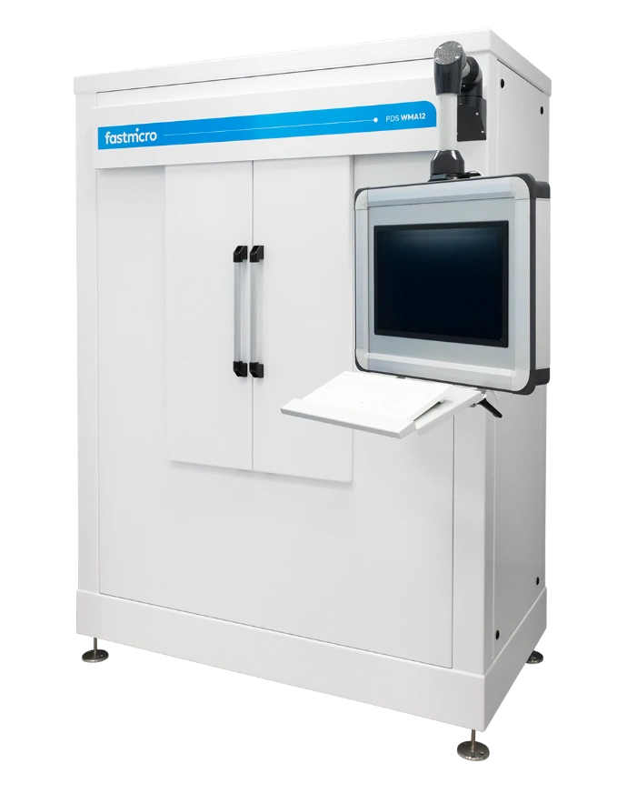
● Systems
PDS-WMA12
Particle Defect Inspection System
for 100 to 200mm wafers, with manual loading interface.
Fastmicro principles.
Why our solutions work