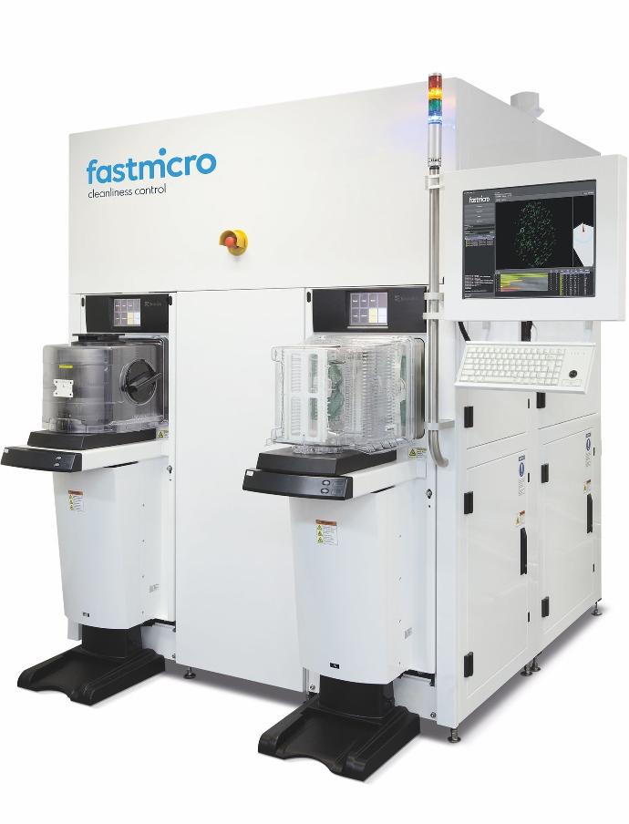
Fastmicro Particle Defect Inspection System | FM-PDS
The Fastmicro Particle Defect Inspection System has been developed to measure surface particle contamination levels directly on a product’s surfaces in any industry down to 100 nm Lower Detection Limit (LDL) at very fast throughput speeds. The primary applications are in Semiconductor (pellicles, reticles, wafers) and the display market. The scanning area is expandable to very large surfaces, like LCD substrates due to its modular and scalable design.
The scanner module is also available as a white label OEM solution for system integrators.
400 WPH Particle Defect Inspection of 12 inch Wafers
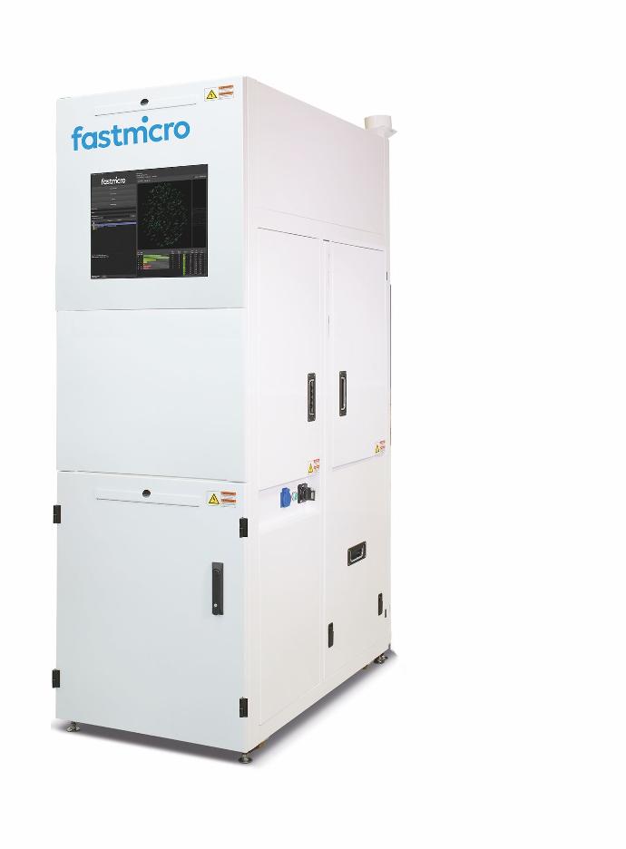
System Specifications
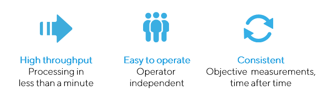
Production Throughput : Capable of 400 Wafers-Per-Hour (WPH)
Analysis : Quantity, Location and Size of particles
Reporting : Qualification report in UI or PDF, acc. to ISO-14644-9
Data output
: KLARF, XML, Excel & Text files (incl standard bin sizes)
Detection limit : Capable from 100 nm PSL particles and up
Reproducibility : 99% cumulative particle count standard particles
Sizing accuracy : Within 20% PSL particles
Location accuracy : 40 um accuracy, 15 um location repeatability
Top/Bottom inspection : Single measurement / No flipping
Control : Fully digital controlled devicenet-ethernet, SECS/GEM
8 inch
Manual
FM-WM8-PDS-V01
- Configurable substrate sizes 100 / 150 / 200 mm
-
Manual loader
- Footprint: 1335x660x2047mm [LxWxH]
8 inch
Automated
FM-WA8-PDS-V01
- Configurable substrate sizes 100 / 150 / 200 mm
- 2 integrated Cassette Stations or SMIF's
- Footprint: 1335x1320x2047mm [LxWxH]

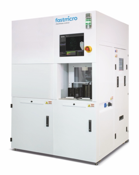
12 inch
Manual
FM-WM12-PDS-V01
- Configurable substrate sizes 150 / 200 / 300 mm
- Manual loader
- Footprint: 1602x755x2099mm [LxWxH]
12 inch
Automated
FM-WA12-PDS-V01
- Configurable substrate sizes 150 / 200 / 300 mm
- 2 FOUP loaders
- Footprint: 1510x1602x2099mm [LxWxH]
The FM-PDS OEM metrology module is available for system integrators and OEM manufacturers. Contact Fastmicro for more information and options.
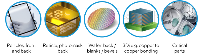
Applications
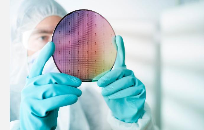
The Fastmicro Particle Defect Inspection System (PDIS) can be used for measurements of:
- Pellicles (front and backside)
- Reticles, photomasks (backside)
- 4 / 6 / 8/ 12 inch Wafers (backside, blanks, bevels)
- 3Di (e.g. copper to copper bonding)
- High Purity Critical parts
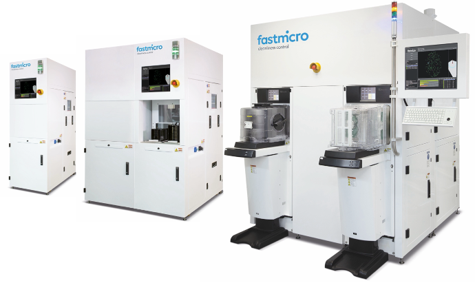
Manual and Automated modular:
Fit for each production process
The modular Fastmicro Particle Defect Inspection System can be customized to suit each production qualification process or to fit into a production line. This can include clean and automated handling: package openers for inspection and cleaning, filling stations, robot arms, an inspection spot and a port for cleaning.
The Fastmicro module allows for a scaled inspection surface to suit customer needs, without introducing extra imaging time and using limited floor space.
Are you ready for the next step in cleanliness control?