
Fastmicro Launches the FM-PDS, a Record-Setting Particle Defect Inspection System Capable of 400 Wafers-Per-Hour and Detecting Particle Sizes Down to 100 nm, Slashing Metrology Throughput Times for In-Line Particle Contamination Monitoring and Control
Fastmicro B.V. announces a revolutionary dark field Particle Defect Inspection System: the FM-PDS product range. The new multi-application metrology platform is designed to create breakthroughs in high-throughput particle inspection down to 100 nm Lower Detection Limit (LDL) of 4-6-8-12-inch Wafers, EUV Pellicles and Reticles, and other critical components requiring high-purity cleanliness. With the 400 Wafer-Per-Hour (WPH) capability of the FM-PDS, customers can rapidly generate primary inspection data at every process step enabling continuous particle contamination monitoring and control of wafers, tools, parts, and overall fab cleanliness.
Smart Manufacturing improving fab yield and eco-footprint
For smart fabs aiming to enhance yield* —a move that also directly affects eco-footprints— the next step involves generating more detailed particle defectivity data and cleanliness indicators. This data, combined with intelligent scheduling and AI processing, allows for automated optimization. However, defectivity inspection time budgets are under pressure due to the increasing total workflow complexity at advanced nodes. The use of the FM-PDS tool, with its fast inspection speed, allows fabs to rethink the business case calculus for metrology strategies. These strategies could include full 100% inspection, or the addition or replacement of ageing particle inspection tools at- or in-line at production. *Source: Next Steps For Improving Yield (semiengineering.com)
Particle inspection applications
The Fastmicro Particle Defect Inspection System measures cumulative particle count, size, and location to provide particle contamination monitoring as set by user-defined recipes or SCP cleanliness classification according to the ISO14644-9 standard, which is used in high-purity clean systems manufacturing. The FM-PDS distinct technology platform is capable of a Lower Detection Limit of 100 nm (0.1 µm) of standard-sized particles and up on various substrates, such as Si, SiC, GaN, Sapphire and Glass transparent wafers. For EUV Pellicles and Reticles, the system is suitable for defect classification, Top-Bottom distinction, and Pinhole confidence classification. More granular primary inspection data can be used to reduce overall particle defectivity, provide detection of data-drift and to optimize fab yield excursions. It also provides insights into tool cleaning and part maintenance needs, resulting in improved tool utilization and downtime optimization.
Modular system, fixed-FOV metrology
The modular FM-PDS particle defect inspection system can be configurated for both top- and bottom-side scanning in a single cycle, without physically moving the product or having to move parts in metrology. Through its fixed Field-Of-View (FOV) optics, the system is uniquely stable, generates a minimum of particles, and keeps up with the highest in-line production cycle times.
With a principal image capturing capability of over 400 Wafers-Per-Hour (WPH) for 4-6-8-inch, and 12-inch wafer sizes, the FM-PDS delivers high-speed inspection capability, unmatched by any other dark field defect inspection system on the market. Thanks to the fast imaging, the automated system can benefit from future innovations in maximum wafer loading speeds made possible by equipment front-end module (EFEM) suppliers.
Fastmicro has developed the FM-PDS product range from the ground up and it incorporates multiple patent-pending breakthrough technologies, reflecting years of research and development ‘Innovated by TNO’ for the Dutch EUV Lithography ecosystem of ultra-clean high-tech systems manufacturing.
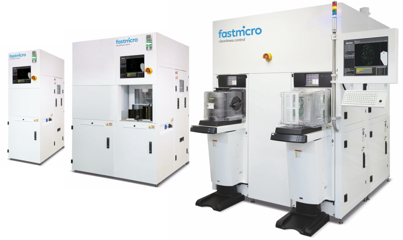
The Fastmicro Particle Defect Inspection System is available in various configurations:
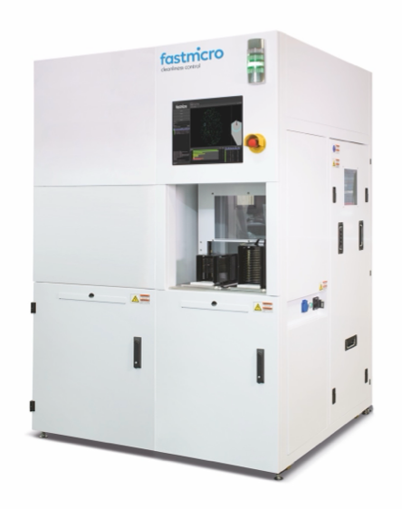
- FM-WM-PDS: Manual 4-6-8-inch wafer and a 12-inch wafer version that can be used with Manual Cassette Stations or SMIFs loaders, also used in Academic- and R&D-labs.
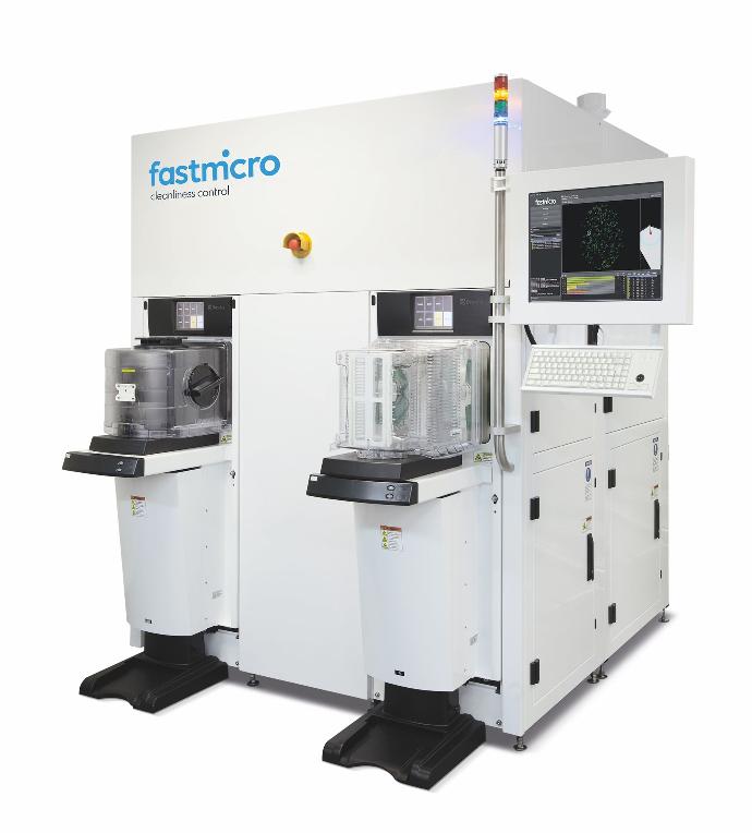
- FM-WA-PDS: fully Automated in-line 4-6–8-inch wafer that can be configured for either 2 to 4 Cassette Stations or SMIF loaders and the 12-inch wafer version with two FOUP loaders. These systems will be equipped with SECS/GEM integration and on customer specification with GEM300/EDA Smart Factory automation providing distributed metrology data exchange.
- FM-PR-PDS: Pellicle and Reticle inspection system with optional top- and bottom-side particle and defect inspection, meeting vibration-free handling requirements by Photomask shops.
- FM-OEM-PDS: metrology module for system integrators and OEM manufacturers.
Erik Vermeulen, CEO of Fastmicro B.V. comments, “With the ultra-fast particle inspection that the FM-PDS offers, Fastmicro has raised the dark field particle inspection technology performance level to a new industry benchmark. Previously, particle defect inspection systems have not matched the required cycle-time speeds that modern DUV and EUV Lithography systems offer to enable 100% in-line particle defect inspection at every step in the flow.” Erik continues, “The increasing complexity of leading-edge process flow steps puts pressure on metrology time budgets. This forces process and yield-control managers to make trade-offs between yield improvement vs. defect inspection.
Utilizing the granular inspection data enabled by the FM-PDS, traditional defect control strategies and business cases can be re-evaluated to further develop Smart Manufacturing and AI Metrology Scheduling strategies.” Erik concludes, “Fastmicro believes that fast particle contamination control is the key to address the Semiconductor industry estimated 30 billion US$ global annual yield loss and the directly linked sustainability challenges, caused by the increasing effects of particle contamination and related defectivities.”
The first Fastmicro Particle Defect Inspection System is in operation at a launching OEM customer in the Dutch EUV Lithography ecosystem, where the system has transformed the inspection capability of Pellicles significantly. Inspection of EUV Pellicles is challenging due to reduced thickness and the more translucent advanced materials being used. The FM-PDS excellent location accuracy enables a more efficient workflow for follow-up root-cause analysis with a high-end microscope as implemented in this case.
Launching Customer Endorsement:
“Fastmicro has enabled us to significantly speed up our testing and development process by reducing our measurement time by a factor 9.”
ASML, Imre Dehner, MSc., Main Delivery Owner Pellicle Defectivity
Optimized Metrology Workflow
The FM-PDS provides efficiency optimization for follow-up particle defect characterization in combination with narrow Field-of-View (FOV), SEM, TEM, and other metrology tools. The system provides fast defect mapping and pathfinding, reducing overall metrology cycle times and making optimal use of scarce in-line resources.
Additional information about the new Fastmicro Particle Defect Inspection System can be found on the FM-PDS product page.
For press or product inquires; please use the form below: