The Fastmicro Particle Defect Inspection System has been developed to measure surface particle contamination levels directly on a product’s surfaces in any industry down to 200 nm Lower Detection Limit (LDL) at very fast throughput speeds. The primary applications are in Semiconductor (pellicles, reticles, wafers) and the display market. The scanning area is expandable to very large surfaces, like LCD substrates due to its modular and scalable design.
The scanner module is also available as a white label OEM solution for system integrators.
Particle Defect Inspection Systems
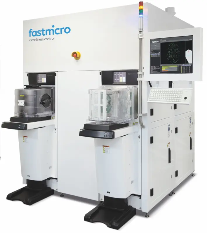
8-inch Automated
FM-WA8-PDS-V01
Configurable substrate sizes:
100 / 150 / 200 mm
2 integrated Cassette Stations or SMIF's
Footprint:
1335x1320x2047mm [LxWxH]
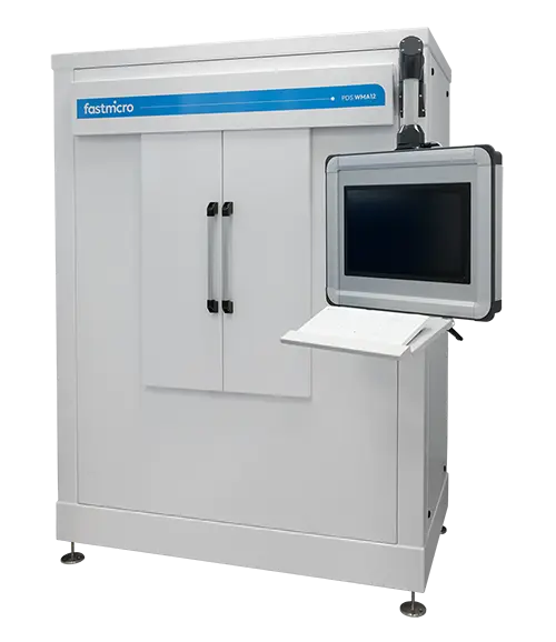
12-PDS-V01
Configurable substrate sizes:
150 / 200 / 300 mm
Manual loader
Footprint:
1602x755x2099mm [LxWxH]
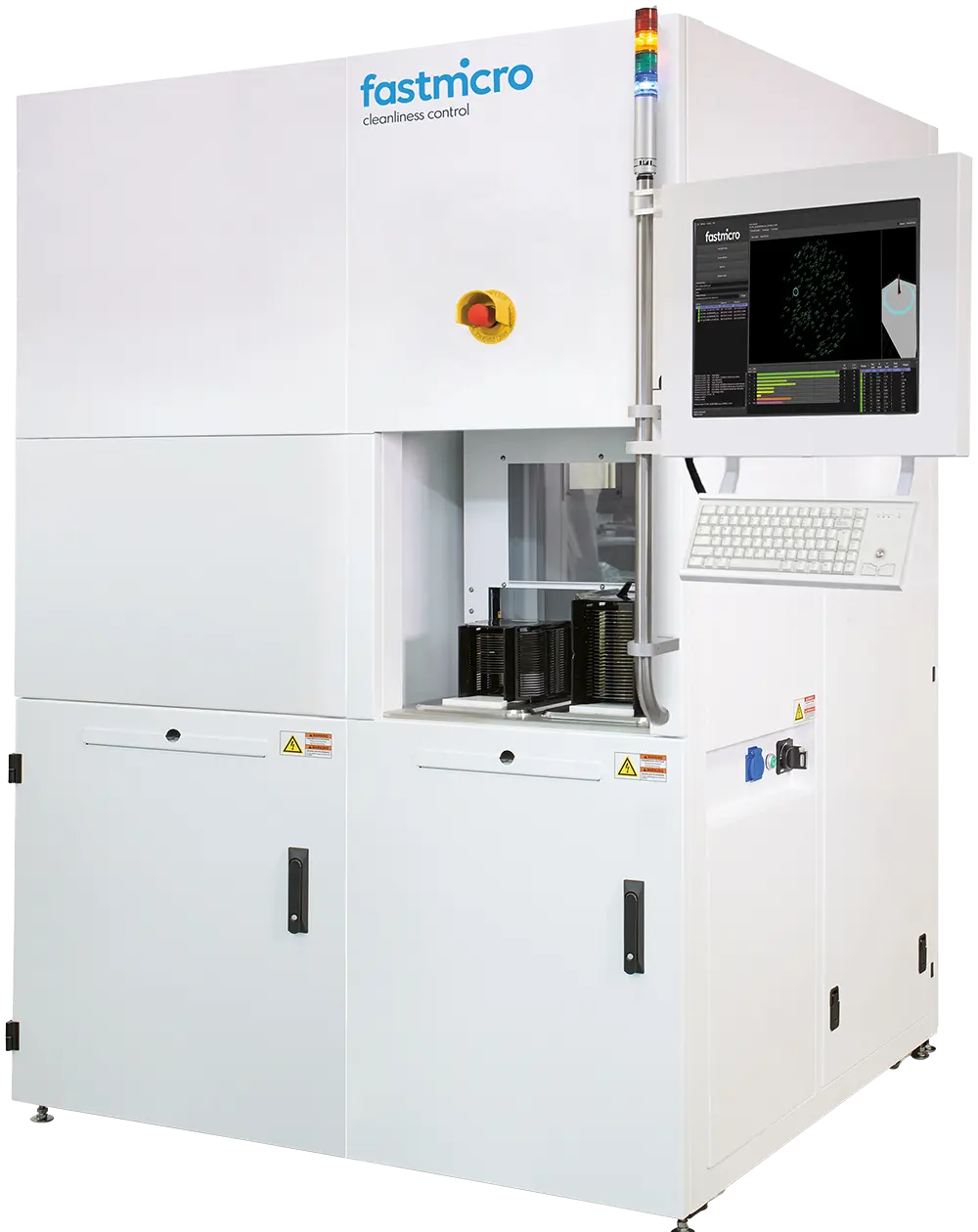
12-inch Automated
FM-WA12-PDS-V01
Configurable substrate sizes:
150 / 200 / 300 mm
2 FOUP loaders
Footprint:
1510x1602x2099mm [LxWxH]

8-inch Manual
FM-WM8-PDS-V01
Configurable substrate sizes:
100 / 150 / 200 mm
Manual loader
Footprint:
1335x660x2047mm [LxWxH]
The Fastmicro Particle Defect Inspection System Applications
PDS can be used for particle measurements on:
- Up to 400 wafers/hour
- No moving or rotating wafer stage
- Simultaneous front & back side inspection
- Compatible with silicon, compound, glass wafers, pellicles, reticles
- High depth of focus
- No degradation of sensitive photoresist layers
- Replace multiple legacy systems with one .
- Pre-scan for follow up analysis
- Current sensitivity 200 nm
- Supports manual and automated processing for up to 12-inch wafers
- Multi-product recipes and interfaces available
High Purity Critical parts
3Di
copper to copper
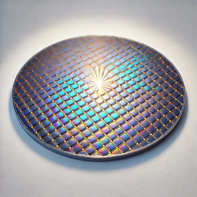
WAFERS
backside blanks bevels
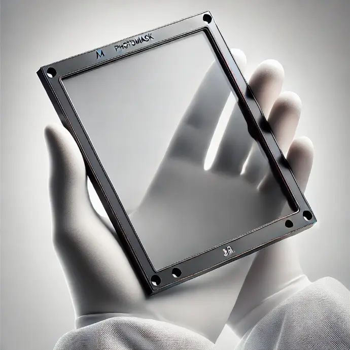
RETICLES
photomasks backside
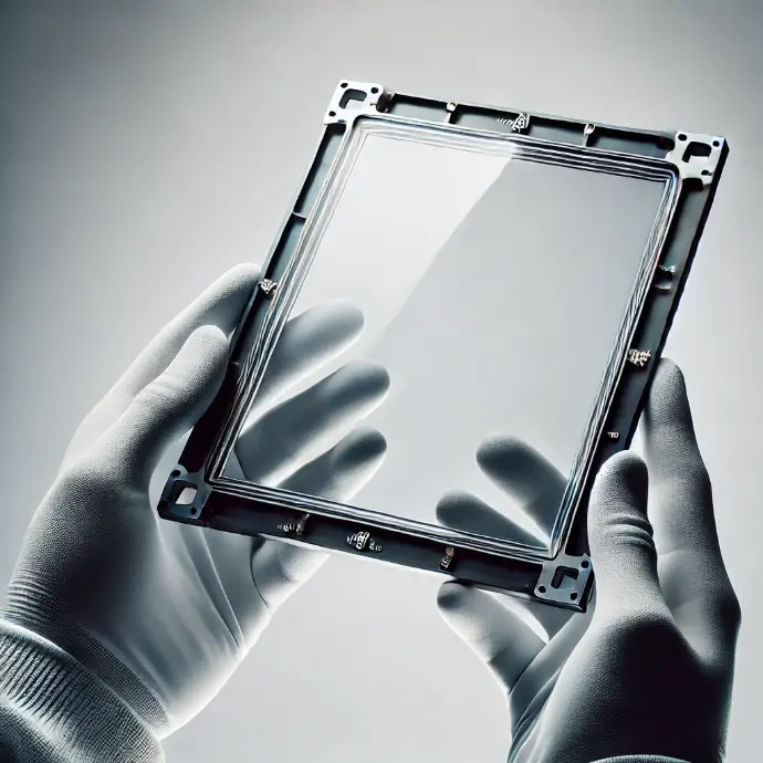
PELLICLES
front and backside

FAST

QUANTITATIVE

EASY TO OPERATE

ACCURATE

CONSISTENT

HIGH THROUGHPUT
Contact us
about anything related to our Particle Defect Inspection Systems.