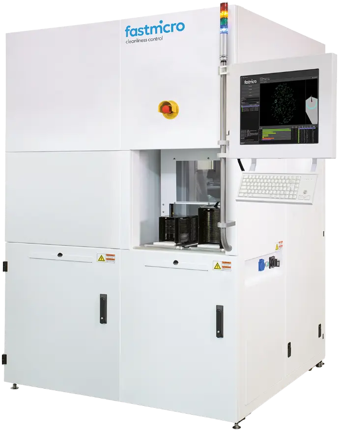
Wafer Particle
Defect Inspection System
Manual and Automated for 4-, 6-, 8- and 12-inch wafers.
Detection Rage from 0.1 µm PSL particles
High-throughput up to 400 Wafer Per Hours (WPH)
Location accuracy 40 µm, location repeatability 15 µm

FAST

QUANTITATIVE

EASY TO OPERATE

ACCURATE

CONSISTENT

HIGH THROUGHPUT
FM-PDS: multi-application modular platform
The modular Fastmicro Particle Defect Inspection System metrology platform can be customized to suit each production qualification process or to fit into a production line. This can include manual and automated wafer handling: package openers for inspection and cleaning, filling stations, robot arms, an inspection spot and a port for cleaning.
The Fastmicro system allows for a scaled inspection surface to suit customer needs, without introducing extra imaging time and using limited floor space.
Direct measurements on product surface
The Fastmicro Particle Defect Inspection System has been developed to measure surface particle contamination levels directly on a product surface in any industry. The primary applications are wafer, pellicles and reticles inspection in Semicon, but also substrates, like in the display market.
The Particle Defect Inspection System has a 4 to 12-inch FOV scanning area, with top- & -bottom-side capability, without moving the product in the metrology stage due to its distinct optics design.
The system can be customized, depending on the the surface that needs to be tested. The metrology module is also available as a white label solution for system integrators and OEM’s.
Wafer PDS Applications
High Purity Critical parts
3Di
copper to copper
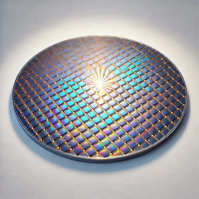
WAFERS
backside blanks bevels
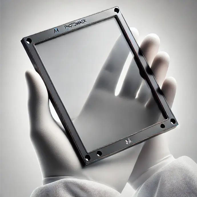
RETICLES
photomasks backside
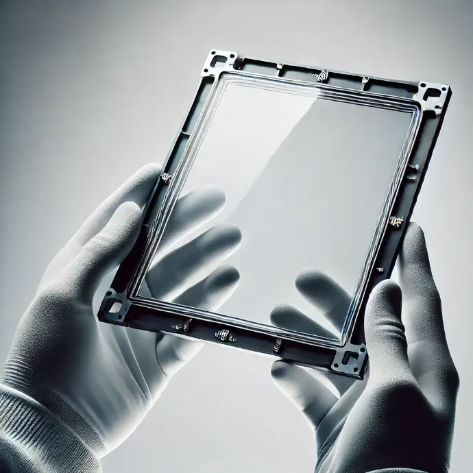
PELLICLES
front and backside
Contact Us Now
about anything related to our Wafer Defect Inspection.